- 您现在的位置:买卖IC网 > Sheet目录2008 > MAX1245BCPP (Maxim Integrated Products)IC ADC SRL 12BIT 2.375V 20-DIP
MAX1245
+2.375V, Low-Power, 8-Channel,
Serial 12-Bit ADC
10
______________________________________________________________________________________
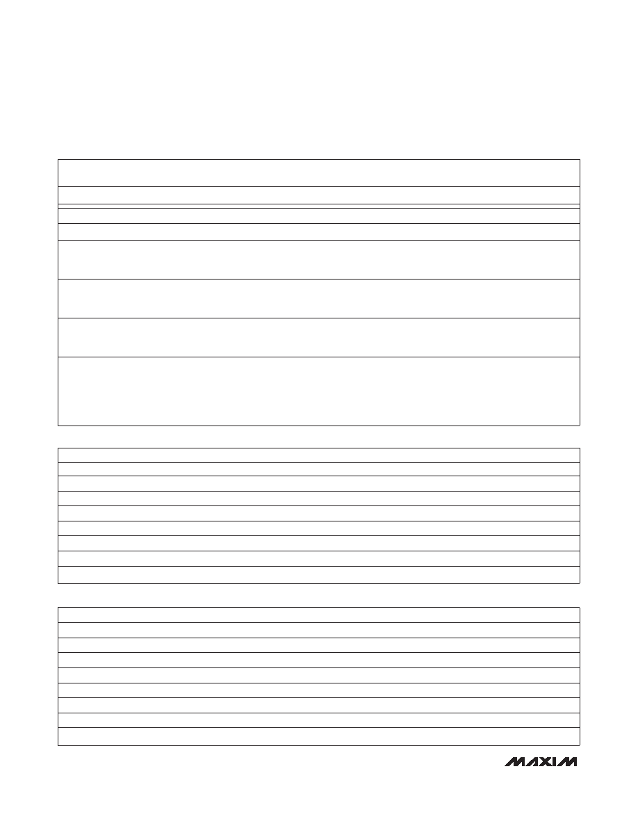
BIT 7
BIT 6
BIT 5
BIT 4
BIT 3
BIT 2
BIT 1
BIT 0
(MSB)
(LSB)
START
SEL2
SEL1
SEL0
UNI/BIP
SGL/DIF
PD1
PD0
BIT
NAME
DESCRIPTION
7(MSB)
START
The first logic “1” bit after CS goes low defines the beginning of the control byte.
6
SEL2
These three bits select which of the eight channels are used for the conversion (Tables 2 and 3).
5
SEL1
4
SEL0
3
UNI/BIP
1 = unipolar, 0 = bipolar. Selects unipolar or bipolar conversion mode. In unipolar mode, an
analog input signal from 0V to VREF can be converted; in bipolar mode, the signal can range
from -VREF/2 to +VREF/2.
2
SGL/DIF
1 = single ended, 0 = differential. Selects single-ended or differential conversions. In single-
ended mode, input signal voltages are referred to COM. In differential mode, the voltage
difference between two channels is measured (Tables 2 and 3).
1
PD1
Selects clock and power-down modes.
0(LSB)
PD0
PD1
PD0
Mode
0
Power-down (IQ = 1.2A)
0
1
Unassigned
1
0
Internal clock mode
1
External clock mode
Table 1. Control-Byte Format
SEL2
SEL1
SEL0
CH0
CH1
CH2
CH3
CH4
CH5
CH6
CH7
COM
00
0
+
–
10
0
+
–
00
1
+
–
10
1
+
–
01
0
+
–
11
0
+
–
01
1
+–
11
1
+
–
Table 2. Channel Selection in Single-Ended Mode (SGL/D
DIIF
F = 1)
SEL2
SEL1
SEL0
CH0
CH1
CH2
CH3
CH4
CH5
CH6
CH7
00
0
+
–
00
1
+
–
01
0
+
–
01
1
+–
10
0
–
+
10
1
–
+
11
0
–
+
11
1
–+
Table 3. Channel Selection in Differential Mode (SGL/D
DIIF
F = 0)
发布紧急采购,3分钟左右您将得到回复。
相关PDF资料
MAX1249AEPE+
IC ADC 10BIT SERIAL 16-DIP
MAX1279AETC+
IC ADC 12BIT 1.5MSPS 12-TQFN
MAX1285BESA+T
IC ADC 12BIT 300KSPS 8-SOIC
MAX1302BEUG+
IC ADC 16BIT SRL 115KSPS 24TSSOP
MAX1303BEUP+
IC ADC 16BIT MULT RANGE 20TSSOP
MAX1308ECM+T
IC ADC 12BIT 8CH 4MSPS 48LQFP
MAX1320ECM+T
IC ADC 14BIT 8CH 2MSPS 48LQFP
MAX132EWG+T
IC ADC 18BIT SERIAL 24-SOIC
相关代理商/技术参数
MAX1245BCPP+
功能描述:模数转换器 - ADC 10-Bit 8Ch 100ksps 3.3V Precision ADC RoHS:否 制造商:Texas Instruments 通道数量:2 结构:Sigma-Delta 转换速率:125 SPs to 8 KSPs 分辨率:24 bit 输入类型:Differential 信噪比:107 dB 接口类型:SPI 工作电源电压:1.7 V to 3.6 V, 2.7 V to 5.25 V 最大工作温度:+ 85 C 安装风格:SMD/SMT 封装 / 箱体:VQFN-32
MAX1245BEAP
功能描述:模数转换器 - ADC Integrated Circuits (ICs) RoHS:否 制造商:Texas Instruments 通道数量:2 结构:Sigma-Delta 转换速率:125 SPs to 8 KSPs 分辨率:24 bit 输入类型:Differential 信噪比:107 dB 接口类型:SPI 工作电源电压:1.7 V to 3.6 V, 2.7 V to 5.25 V 最大工作温度:+ 85 C 安装风格:SMD/SMT 封装 / 箱体:VQFN-32
MAX1245BEAP+
功能描述:模数转换器 - ADC 10-Bit 8Ch 100ksps 3.3V Precision ADC RoHS:否 制造商:Texas Instruments 通道数量:2 结构:Sigma-Delta 转换速率:125 SPs to 8 KSPs 分辨率:24 bit 输入类型:Differential 信噪比:107 dB 接口类型:SPI 工作电源电压:1.7 V to 3.6 V, 2.7 V to 5.25 V 最大工作温度:+ 85 C 安装风格:SMD/SMT 封装 / 箱体:VQFN-32
MAX1245BEAP+T
功能描述:模数转换器 - ADC 10-Bit 8Ch 100ksps 3.3V Precision ADC RoHS:否 制造商:Texas Instruments 通道数量:2 结构:Sigma-Delta 转换速率:125 SPs to 8 KSPs 分辨率:24 bit 输入类型:Differential 信噪比:107 dB 接口类型:SPI 工作电源电压:1.7 V to 3.6 V, 2.7 V to 5.25 V 最大工作温度:+ 85 C 安装风格:SMD/SMT 封装 / 箱体:VQFN-32
MAX1245BEAP-T
功能描述:模数转换器 - ADC RoHS:否 制造商:Texas Instruments 通道数量:2 结构:Sigma-Delta 转换速率:125 SPs to 8 KSPs 分辨率:24 bit 输入类型:Differential 信噪比:107 dB 接口类型:SPI 工作电源电压:1.7 V to 3.6 V, 2.7 V to 5.25 V 最大工作温度:+ 85 C 安装风格:SMD/SMT 封装 / 箱体:VQFN-32
MAX1245BEPP
功能描述:模数转换器 - ADC RoHS:否 制造商:Texas Instruments 通道数量:2 结构:Sigma-Delta 转换速率:125 SPs to 8 KSPs 分辨率:24 bit 输入类型:Differential 信噪比:107 dB 接口类型:SPI 工作电源电压:1.7 V to 3.6 V, 2.7 V to 5.25 V 最大工作温度:+ 85 C 安装风格:SMD/SMT 封装 / 箱体:VQFN-32
MAX1245BEPP+
功能描述:模数转换器 - ADC 10-Bit 8Ch 100ksps 3.3V Precision ADC RoHS:否 制造商:Texas Instruments 通道数量:2 结构:Sigma-Delta 转换速率:125 SPs to 8 KSPs 分辨率:24 bit 输入类型:Differential 信噪比:107 dB 接口类型:SPI 工作电源电压:1.7 V to 3.6 V, 2.7 V to 5.25 V 最大工作温度:+ 85 C 安装风格:SMD/SMT 封装 / 箱体:VQFN-32
MAX1245BMJP
功能描述:模数转换器 - ADC RoHS:否 制造商:Texas Instruments 通道数量:2 结构:Sigma-Delta 转换速率:125 SPs to 8 KSPs 分辨率:24 bit 输入类型:Differential 信噪比:107 dB 接口类型:SPI 工作电源电压:1.7 V to 3.6 V, 2.7 V to 5.25 V 最大工作温度:+ 85 C 安装风格:SMD/SMT 封装 / 箱体:VQFN-32